

Flat Optical Components and Flat Optics. 1/4 Wave Optical Polishing Services, Filled Via Polishing Service. Thin Sapphire Window, Ultra Thin Wafers and Substrates. Thin Sapphire Wafers and Substrates The thinnest Sapphire wafers and parts can be made from A-plane Sapphire [1120] orientation.
Thickness of 25 microns (0.0009") has been achieved. Stainless Steel 17-4 PH polished optical mirrors. Superpolished Stainless Steel Optics and Mirrors Superpolished metal surfaces approaching 5 Angstrom Ra finish, without using polished electroless nickel plating are now possible for use as mirrors.
Valley's process of optically polishing these pure metal substrates and wafers enables materials such as 304SS, 316SS, 430SS and 17-4 PH (Custom 630) Stainless Steel, to be used as mirrors. Physical properties of 17-4 PH Stainless Steel which are important for critical applications include: High-strength steel alloy Composition percentages: C = 0.07, Mn = 1.0 max, Ni = 3.0 - 5.0, Cu = 3.0 - 5.0, Nb + Ta = 0.15 - 0.45, Fe = balance Safe, continuous operating temperature: 316°C (600°F) Thermal conductivity: 17.9 W/mK CTE: 10.8 x 10⁻⁶ at 100°C Density: 7.75 g/cc. Contract Lapping and Polishing Services at Very Low Cost. Polished Polyimide Wafers & Substrates. 304 Stainless Steel Properties, Melting Point Of 304 Stainless Steel. Type 304 and 304 L Stainless Steel 304 Stainless Steel (SS) is an austenitic stainless steel with Face Centered Cubic (F.C.C.) atomic structure which provides numerous planes for the movement of dislocations.
This inherent property, combined with the low level of interstitial elements (elements which lack the dislocation chain), gives this material high ductility, low yield stress and relatively high ultimate tensile strength. As steel is heated above critical temperature (approx. 1335 F) it undergoes a phase change, recrystallizing as austenite. Continued heating to approx. 1450 - 1500F assures complete conversion to austenite.
Polished ceramic substrates of alumina and AlN. Polished and Lapped Ceramic Substrates Polished ceramic, quartz, high dielectric, sapphire, glass, fused silica, AlN and numerous other hard materials can be shipped from stock.
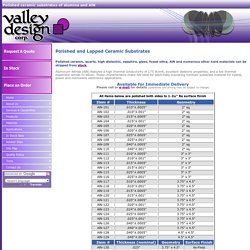
Aluminum Nitride (AlN) features a high thermal conductivity of 175 W/mK, excellent dielectric properties, and a low thermal expansion similar to silicon. These characteristics make AlN ideal for electrically insulating nontoxic substrate material for hybrid, power and microwave electronics applications. Available for Immediate Delivery Please call or e-mail for details (quantities and pricing may be subject to change) Aluminum Nitride AlN Lapped Substrates 175 W/mk Note: For tighter tolerances and better surface finish, please contact Customer Service at 831.420.0595.
Contract Lapping and Polishing Services at Very Low Cost. Single Crystal Quartz Machining. Best Stainless Steel Wafer Polishing Services. Polished Stainless Steel Wafers Stainless steel wafers and substrates are now available from Valley in lapped or polished surface finishes.
Stainless Steel wafers and substrates may be used for various applications such as solar cells, thick film circuitry, heaters, and for many R&D and medical applications. SS wafers are available in standard SEMI diameters with various finishes ranging from a few Angstroms to rough machined surfaces, and in all thicknesses from as thin as 25um up to large thick vacuum chucks. Standard wafer thicknesses are 50um, 125um, 250um, 500um, 1mm and thicker. Commonly available surface finishes for these Stainless Steel wafers and substrates include: As-machined Abrasive lapped Diamond lapped Buffed Fine buffed Polished Fine polished Optically polished.
Polished Aluminum Nitride (ALN) Wafers, Lapped Alumina Polishing. Polished and Lapped Ceramic Substrates Available. Synthetic Sapphire Polishing Services, Sapphire Lapping Service. Polyimide Substrates, Unfilled Polyimide Applications Properties. 304 Stainless Steel Properties, Melting Point Of 304 Stainless Steel. Ultrasonic Drilling Ceramic Service and Thin Substrates. Thin Substrate and Wafer Hole Drilling and Coring Ultra-thin material hole drilling, core drilling and dicing has been a specialty at Valley design for close to 40 years.
Soda Lime Glass Wafers Properties. Buy Polished Sapphire Wafers and Substrates Online. Polished Polyimide Wafers & Substrates. Best Stainless Steel Wafer Polishing Services. Ultra Thin Silicon Wafers and MEMS. MEMS Thinning MEMS Micro Electro-Mechanical Systems can contain small mechanical, optical and electronic elements produced by litographic techniques.
Valley stocks and processes many of the materials, including ultra thin, for use in these applications. Silicon-Direct-Bonding (SDB) or Wafer-Direct-Bonding (WDB) also referred to as Fusion Bonding is accomplished when smooth and flat Silicon surfaces are brought together at high temperature. High quality surface finishes (<10A), when required, are provided by Valley Design. Anodic Bonding, also referred to as Electrostatic Bonding, is a process where glass to Silicon or a metal is permanently attached with an irreversible chemical bond. SOI Silicon-On-Insulator refers to a thin layer of Silicon on top of an insulating layer such as glass or Silicon Oxide. For answers to your complex technology needs, come to the company that has been a leader in advanced and ultra thin materials processing for nearly 30 years. Flat Optics. Precision Shims Spacers, Rings, Washers Sized to Micron Levels. Precision Shims Spacers, Rings, Washers Sized to Micron Levels Precision shims spacer and submount components from Valley Design with accurate pitch tolerances and sequentially spaced to less than 1/4 micron, flat to less than 1/10 wave, with lapped or polished mirror finishes available.

Precision glass spacers, shims, submounts, rings, washers, and blocks can be manufactured from many various materials. Shims of all sizes, thicknesses, and surface finishes can be precisely manufactured to your specifications for a variety of applications. Even Heat Kiln Equipment for Sale. Equipment for Sale - Used EvenHeat Kiln Valley Design has an EvenHeat kiln for sale in used condition.
We sell equipment such as lapping machines, ovens, kilns, air gauges, lasers, laser power meters, and 100mm wafer scribers. This particular EvenHeat kiln is being sold in as-is condition, and the buyer must make arrangements to pick up EvenHeat kilns upon completing the purchase. EvenHeat 4320 is a manual model with temperature capability up to 2300 degrees Fahrenheit. Dicing sapphire wafers and sapphire substrates. Fused Quartz Wafers, Fused Quarts Silica Tubing. Fused Quartz Optical Properties The type of manufacturing method and the raw materials used dictate the final properties of the fused quartz produced.

The degree of transparency reflects the material purity. The UV cutoff ranges from about 155 to 175 nm for fused quartz, and is an indicator of material purity. In the IR range, the infrared transmission extends to approximately 4 micrometers with little absorption at 2.73 micrometers (the water band). This means that the quartz is electrically fused, rather than flame fused (or "wet" quartz). Sapphire Thermal Conductivity. Polished R-plane Sapphire Wafers for SOS Valley Design offers thinning and polishing services on customer supplied SOS wafers. R-plane Sapphire (1-102), 57.6 degrees to C-plane, is the preferred material for Silicon-on-Sapphire used in semiconductor, microwave and pressure transducer applications.
Typical applications for Silicon on Sapphire wafers include: Fabrication of active topside Silicon-based devices Fabrication of topside laser devices Backside polishing of the SOS wafer to fabricate an optical device on the Silicon side Etching off the Silicon side to utilize the Sapphire as a SEMI standard wafer, or wafer carrier Valley provides backthinning services to thin SOS wafers to as thin as 125um thick. Polished Polyimide Wafers & Substrates. Custom Optical Coatings and Thin Film Coatings. Metallic optics mirrors vs. metal optics mirrors. Metal Optics Replace Metal Coated Substrates The primary function of an optical mirror is to redirect light. The mirror should be flat, smooth, and provide a durable, stable and easy-to-clean surface. For many applications, a mirror's ability to conduct heat is also extremely important. Common metallic optics mirrors have an Aluminum or Gold coating on various substrate materials of glass, Fused Silica or Fused Quartz.
Left unprotected, Aluminum and Gold mirror coatings are extremely delicate and cannot withstand much cleaning. Using its proprietary technology, Valley Design can now produce Angstrom level optical surface finishes on these pure metal mirrors, eliminating the necessity for expensive and lower performance metallic coatings. Please call or e-mail for more details, or for a quotation per your specifications. Single Crystal Quartz Machining. Corning Fused Silica Wafers & Substrate, Corning 7940 & 7980. Fused silica Corning 7940 wafer material has been discontinued by Corning and was replaced by HPFS (High Purity Fused Silica) 7980, which is an ideal material for UV grade Fused Silica wafers. The two fused silica wafer materials are almost identical in composition, properties and transmission, and can be used interchangeably. The material is a high purity synthetic amorphous silicon dioxide which is manufactured by flame hydrolysis.
Some beneficial characteristics include very low thermal expansion coefficient, very good homogeneity with excellent optical properties and exceptional transmittance in the UV range. Principal Uses for UV Fused Silica. 304 Stainless Steel Properties, Melting Point Of 304 Stainless Steel. Thin Ceramics Substrate for Single Layer Chip Capacitors. Polished Thin Precision Optical Glass Windows Thin precision glass products for the electro-optical industry have been referred to as ultra-thin glass, super-thin glass and micro-thin glass. Valley produces all of these thin optics down to a thickness of 1 mil (25 microns).
Other thin products offered by the company are: Sapphire Thermal Conductivity. Contract Lapping and Polishing Services at Very Low Cost. Single Crystal Quartz Machining. Polished Aluminum Nitride (ALN) Wafers, Lapped Alumina Polishing. Fused Silica Wafers & Substrate, Corning 7980 and 7940 Wafers. Aluminum Nitride (AlN) Substrates and Wafers. Precision Shims Spacers, Rings, Washers Sized to Micron Levels. Multispectral Zinc Sulfide (ZnS) Equipment for Sale - Used Ames Pneumatic Measurement Air Gauge. Equipment for Sale - Used Ames Pneumatic Measurement Air Gauge. Edge, Angle-Facet Optical Polishing for Optoelectronics. Sapphire Thermal Conductivity. Polished Polyimide Wafers & Substrates. Ultrasonic Drilling Ceramic Service and Thin Substrates. Molybdenum metal polished mirrors and optics.
Contract Lapping and Polishing Services at Very Low Cost. Edge, Angle-Facet Optical Polishing for Optoelectronics. 1/4 Wave Optical Polishing Services, Filled Via Polishing Service. Polished Aluminum Nitride (ALN) Wafers, Lapped Alumina Polishing. Glass CNC Machining Service Hard Materials. Precision Lapping Service and Precision Polishing Services. Custom flat lapping and precision polishing of all types of materials from a single piece to millions of pieces, on both customer supplied and on our own supplied materials are the specialty of Valley Design. Based on our extensive experience with a wide variety of materials from soft PEEK to various Optical Glasses and Fused Silica, to hard Ceramics and Sapphire, we can provide lapping and polishing services on almost anything. We have developed multitudes of special processes to solve your unique problems as part of the extraordinary service that we provide our customers.
ISO 9001:2015 certified, all our processes have been carefully documented and are repeatable, so that once you have received a quality product from Valley Design that meets your specifications, you can depend on a consistent production throughput. We pride ourselves on being the ultimate source for all your production and precision lapping and polishing requirements. Laser Slag Removing Services. Corning Fused Silica Wafers & Substrate, Corning 7940 & 7980. Ultra Thin Precision Glass for Precision Optics.
Grinding, Lapping and Polishing 450mm Wafers. Lapping and Polishing All Materials. Ceramic Substrates For Electro-Optic Applications. Cleartran TM, Irtran - 2, Clear ZnS. UV, VIS, and IR optical black coatings. Equipment for Sale - Used Ames Pneumatic Measurement. MEMS Bonded Wafer Dicing. Dicing and cutting sapphire wafers and substrates. Colored Optical Glass Filters. Synthetic Sapphire Polishing Services, Sapphire Lapping Service. Single Crystal Quartz Machining. 304 Stainless Steel Properties, Melting Point Of 304 Stainless Steel. Precision CNC machining and custom CNC micromachining services. Full-Service CNC and Manual Ceramic Machining. Ultra Thin Fused Silica Substrates. Fused Silica Fused quartz and Fused Silica polished substrates, plates, windows, sheets and wafers.
Custom sizes with precision optical surface finishes to 10/5, can be shipped in just a few days. Common size windows are in stock. Ultra-thin polished Fused Silica and Fused Quartz substrates 1"square and 2"square are available for immediate delivery from stock. Thicknesses are 0.002" (50 microns), 0.003" (75 microns), 0.004" (100 microns) and 0.005" (125 microns). Other thicknesses in 1" and 2" square configuration available from stock are 0.010", 0.015", 0.020" (0.5 mm), 0.025" and 0.040" (1 mm). 3"(75 mm) diameter and 4" (100 mm) diameter Fused Silica substrates are semifinished and can be completed to any thickness in just a few days.
A surface finish of 20/10 and thickness tolerances of +/- 0.001", 0.0005", 0.0004", 0.0003" and 0.0002" are typically requested. Aluminum Nitride Machining Services.